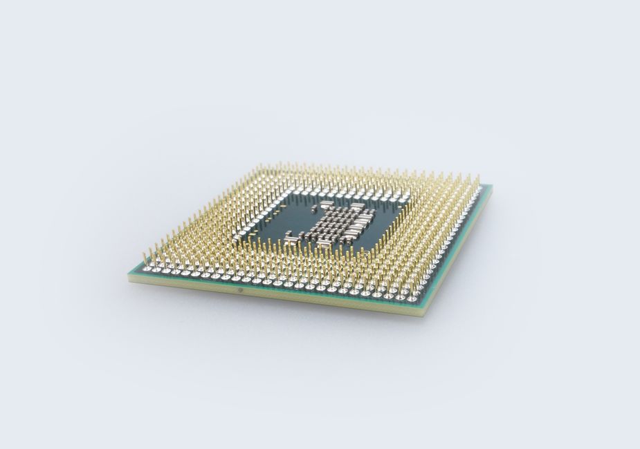
IBM announced on June 25, 2026 a historic achievement in semiconductor engineering: the world’s first sub-1 nanometer chip, packing nearly 100 billion transistors into a space the size of a fingernail. The breakthrough could extend Moore’s Law another decade and reshape AI computing.
The new 0.7 nanometer node delivers up to 50 percent more performance or 70 percent greater energy efficiency than IBM’s 2 nanometer chips, opening the door to vastly more powerful and efficient processors for AI, data centres, and consumer devices.
The Sub-1 Nanometer Achievement
IBM’s announcement {el(“https://newsroom.ibm.com/2026-06-25-ibm-debuts-worlds-first-sub-1-nanometer-chip-technology”,”made public on June 25″)} details a chip at the 0.7 nanometer (7 angstrom) node. The design nearly doubles the transistor density of IBM’s 2 nanometer node, packing more computing power into less space.
This is a significant milestone because the semiconductor industry has long debated whether moving below 1 nanometer was feasible. IBM’s demonstration proves the physics still permits further miniaturisation, challenging predictions that Moore’s Law would stall.
The Nanostack Architecture
The key innovation is called the “nanostack” design, {el(“https://research.ibm.com/blog/sub-1nm-node-chips”,”detailed in IBM’s research blog”)}. Rather than purely horizontal layering, IBM stacks and staggers transistors in a 3D configuration, allowing different material combinations in each layer to optimise performance and power efficiency independently.
This vertical stacking approach squeezes more functionality into the same footprint. Each transistor can now be optimised for its specific job — some for speed, others for power efficiency — rather than forcing a one-size-fits-all compromise.
Performance and Power Gains
The 0.7 nanometer node offers up to 50 percent more performance at the same power budget, or 70 percent greater energy efficiency at the same performance level. For AI workloads that demand both speed and efficiency, the trade-off is valuable.
Energy efficiency is crucial for data centres running large language models and inference workloads. A 70 percent reduction in power consumption would significantly lower cooling costs and electricity bills for cloud providers.
Timeline and Real-World Impact
IBM emphasized the sub-1 nanometer technology is currently a research demonstration. Production is expected around five years away — likely 2031 — which means commercial chips using this node may not reach consumer hands until 2032 or later.
For now, IBM’s 2 nanometer node remains the cutting edge in production. IBM partners with Samsung and TSMC in the advanced chip race, and each breakthrough narrows the gap. The sub-1 nanometer demonstration proves the physics works, paving the way for the next generation of semiconductors.
Related Articles
Qualcomm Acquires AI Startup Modular in $3.9 Billion Deal
Trust Post Desk
A journalist and editor at TrustPost.org covering world and national news, technology updates and human-interest stories. They check every fact, interview sources in person or online, and aim to deliver clear, accurate reporting. Their work ranges from breaking news to in-depth features and daily newsletters. Outside the newsroom, they follow emerging trends and engage with readers on social media.